Notifications

9 minutes, 28 seconds
-327 Views 0 Comments 0 Likes 0 Reviews

The world of electronics has evolved dramatically over the years, with innovations leading to smaller, faster, and more efficient devices. One significant advancement in this area is the development of High-Density Interconnect (HDI) Printed Circuit Boards (PCBs). These specialized PCBs are engineered to offer superior performance in compact electronics design, making them essential for industries ranging from consumer electronics to telecommunications. In this blog post, we'll explore how HDI PCBs are transforming the landscape of compact electronics and why they are crucial for the future of modern technology.
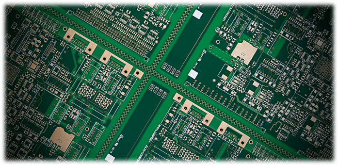
HDI PCBs are a type of circuit board designed with a higher component density than traditional PCBs. This means they can accommodate more components in a smaller area. HDI PCBs feature finer traces, micro vias (smaller vias that connect layers), and higher layer counts compared to conventional boards. These characteristics allow HDI PCBs to provide enhanced electrical performance while maintaining a compact size. As technology continues to shrink, the demand for more efficient and smaller PCBs is growing rapidly. HDI PCBs offer the perfect solution for meeting these demands.
In the realm of compact electronics, space is at a premium. Devices are getting smaller, but they still need to pack powerful features and functionality. HDI PCBs allow designers to maximize the available space on a circuit board by using smaller, more precise components. The ability to fit more circuitry in a smaller space opens up opportunities for creating more compact electronic devices without compromising on performance. Whether you're designing smartphones, wearable devices, or advanced automotive systems, HDI PCBs provide the flexibility to pack more features into a smaller footprint.
The high-density design of HDI PCBs enables faster signal transmission with minimal interference. Their fine trace widths and smaller vias help reduce signal loss and improve the overall performance of electronic systems. As devices become smaller, the importance of maintaining signal integrity grows. HDI PCBs minimize the distance between components, which not only improves speed but also reduces power consumption. These improvements make HDI PCBs ideal for high-performance applications, such as 5G technology, advanced medical devices, and high-speed data transmission systems.
The manufacturing process for HDI PCBs ensures a higher level of precision and quality, which translates into improved durability and reliability. The smaller and more complex traces in HDI PCBs require high-quality materials and meticulous construction techniques. These factors contribute to making HDI PCBs more robust and able to withstand the harsh conditions often encountered in electronics, such as high temperatures, humidity, and mechanical stress. For industries that rely on mission-critical systems, the superior reliability of HDI PCBs is essential.
While HDI PCBs may have higher initial production costs due to their complexity, they can lead to cost savings in the long term. Their ability to accommodate smaller, more powerful components means that companies can reduce the number of components needed in a design. This reduction can lower assembly and manufacturing costs. Additionally, the smaller size of HDI PCBs enables more efficient use of space in the final product, leading to a reduction in packaging costs. For businesses looking to maintain high-quality standards while keeping production costs manageable, HDI PCBs are an attractive option.
As the demand for smaller, more efficient electronics continues to grow, the need for more advanced PCBs will become even more pronounced. HDI PCBs are at the forefront of this technological evolution. By integrating cutting-edge features like smaller vias and higher layer counts, HDI PCBs are well-equipped to handle the challenges of next-generation devices. Their flexibility allows for greater design freedom, enabling manufacturers to keep pace with the ever-evolving tech landscape.
HDI PCBs are used in a wide variety of compact electronics, ranging from consumer gadgets to specialized industrial equipment. Some of the most common applications include:
As the demand for smaller, more efficient electronics continues to rise, choosing the right PCB is more important than ever. HDI PCBs offer unparalleled space efficiency, enhanced performance, and greater durability, making them the ideal choice for compact electronic devices. Their ability to integrate more components in a smaller footprint allows for the creation of advanced devices that push the boundaries of what is possible in electronic design.
At Pcb-Togo Electronic, Inc., we specialize in the design and manufacturing of HDI PCBs tailored to your specific requirements. Our high-quality PCBs are designed to support the next generation of compact electronics, ensuring your devices stand out in a crowded marketplace. Click this link here now to learn more about our HDI PCB offerings and how we can assist in taking your electronics design to the next level.
HDI PCBs are revolutionizing the way electronics are designed, offering a perfect balance of size, performance, and reliability. As technology continues to advance and the demand for compact, high-performance devices grows, HDI PCBs will remain at the forefront of innovation. Whether you're developing the latest smartphone, wearable tech, or telecommunication system, HDI PCBs provide the versatility and power needed to meet modern design challenges. By embracing HDI PCBs, you can future-proof your electronics and ensure that your products stand out in the competitive tech landscape.
Original Link: https://pcbtogo.blogspot.com/2024/12/how-hdi-pcbs-revolutionize-compact.html

